- 您现在的位置:买卖IC网 > Sheet目录476 > MC44CC375AVEFEVK (Freescale Semiconductor)CCEVK NEJA EVAL KIT
ELECTRICAL SPECIFICATIONS
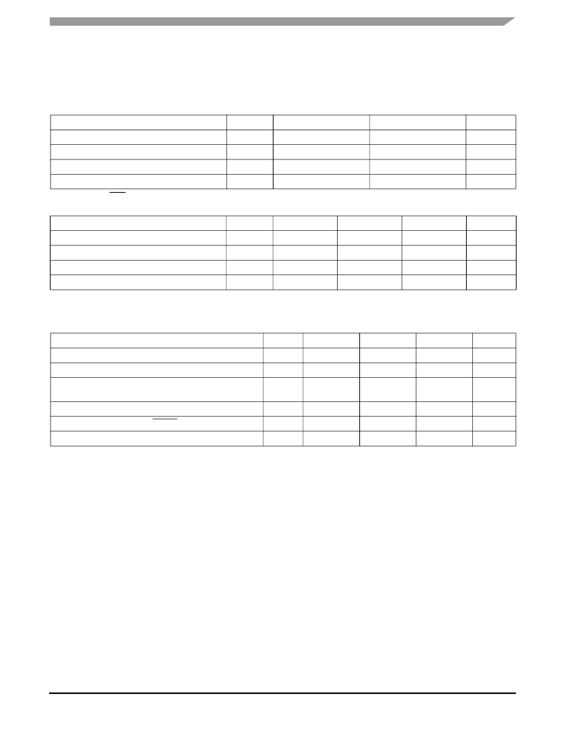
Table 3. Absolute Maximum Ratings
Absolute maximum continuous ratings are those maximum values beyond which damage to the device may occur. Exposure
to these conditions or conditions beyond those indicated may adversely affect device reliability. Functional operation at absolute-
maximum-rated conditions is not implied.
Characteristic
Supply Voltage
Any Input Voltage*
Storage Temperature Range
Junction Temperature
Symbol
V CC
V in
T stg
T J
Min
-0.3
-0.3
-65
—
Max
+3.6
V CC + 0.3
+150
+105
Units
V
V
° C
° C
*Except for Pin 3, SOC.
Table 4. General Specifications
Characteristic
ESD Protection (Charge Device Model)
ESD Protection (Human Body Model) (1)
Latch-up Immunity
Thermal resistance from Junction to Ambient
Symbol
CDM
HBM
LU
R Θ JA
Min
-500
-2000
200
—
Typ
—
—
—
102
Max
+500
+2000
—
—
Units
V
V
mA
°C/W
1. JEDEC JESD22-A114D.
Table 5. Recommended Operating Conditions and DC Characteristics
Characteristic
Supply Voltage
Total supply current (all sections active)
Sound comparator charge pump current:
While locking
Symbol
V CC
I CC
Min
+3
65
1.0
Typ
+3.3
85
3.9
Max
+3.6
98
7.0
Units
V
mA
μ A
RF comparator charge pump current
When locked
—
1.2
1.0
1.6
1.5
2
μ A
mA
Threshold level on pins: CHS, PSAVE,
Ambient Temperature
V th
T A
—
0
2.1
—
—-
+70
V
° C
NOTE: Crystal specification reference information
Frequency = 4 MHz
Mode = Parallel Resonance
Load Capacitance = 27 pF
Motional Resistance = 10 Ohms Typical (100 Ohms Maximum Starting)
MC44CC375AV
Digital Home
Freescale Semiconductor
5
发布紧急采购,3分钟左右您将得到回复。
相关PDF资料
MCH3374-TL-E
MOSFET P-CH 12V 3A MCPH3
MCH3375-TL-H
MOSFET P-CH 1.6A 30V MCPH3
MCH3377-TL-E
MOSFET P-CH 20V 3A MCPH3
MCH3377-TL-H
MOSFET P-CH 3A 20V MCPH3
MCH3382-TL-H
MOSFET P-CH 2A 12V MCPH3
MCH3383-TL-H
MOSFET P-CH 12V 3.5A MCH3
MCH3474-TL-H
MOSFET N-CH 4A 30V MCPH3
MCH3475-TL-E
MOSFET N-CH 30V 1.8A MCPH3
相关代理商/技术参数
MC44CC375AVEFR2
功能描述:调节器/解调器 CMOS MOD R3.0 375AV RoHS:否 制造商:Texas Instruments 封装 / 箱体:PVQFN-N24 封装:Reel
MC44CD02FC
功能描述:IC RECEIVER TUNER 0-IF 48-QFN RoHS:是 类别:RF/IF 和 RFID >> RF 接收器 系列:- 产品培训模块:Lead (SnPb) Finish for COTS 产品变化通告:Product Discontinuation 09/Jan/2012 标准包装:50 系列:* 频率:850MHz ~ 2.175GHz 灵敏度:- 数据传输率 - 最大:- 调制或协议:- 应用:* 电流 - 接收:* 数据接口:PCB,表面贴装 存储容量:- 天线连接器:PCB,表面贴装 特点:- 电源电压:4.75 V ~ 5.25 V 工作温度:0°C ~ 85°C 封装/外壳:40-WFQFN 裸露焊盘 供应商设备封装:40-TQFN-EP(6x6) 包装:托盘
MC44CD02FCR2
功能描述:IC RECEIVER TUNER 0-IF 48-QFN RoHS:是 类别:RF/IF 和 RFID >> RF 接收器 系列:- 产品培训模块:Lead (SnPb) Finish for COTS 产品变化通告:Product Discontinuation 09/Jan/2012 标准包装:50 系列:* 频率:850MHz ~ 2.175GHz 灵敏度:- 数据传输率 - 最大:- 调制或协议:- 应用:* 电流 - 接收:* 数据接口:PCB,表面贴装 存储容量:- 天线连接器:PCB,表面贴装 特点:- 电源电压:4.75 V ~ 5.25 V 工作温度:0°C ~ 85°C 封装/外壳:40-WFQFN 裸露焊盘 供应商设备封装:40-TQFN-EP(6x6) 包装:托盘
MC44CM373CAEF
功能描述:多媒体杂项 CMOS 373CA RoHS:否 制造商:Texas Instruments 类型: 通道数量: 转换速率:540 Mbps 分辨率: 封装 / 箱体:SOIC-16 封装:Tube
MC44CM373CAEFEVK
功能描述:射频开发工具 CMOS MOD EVAL KIT RoHS:否 制造商:Taiyo Yuden 产品:Wireless Modules 类型:Wireless Audio 工具用于评估:WYSAAVDX7 频率: 工作电源电压:3.4 V to 5.5 V
MC44CM373CAEFR2
功能描述:多媒体杂项 CMOS 373CA RoHS:否 制造商:Texas Instruments 类型: 通道数量: 转换速率:540 Mbps 分辨率: 封装 / 箱体:SOIC-16 封装:Tube
MC44CM373CASEF
功能描述:调节器/解调器 CMOS MOD R2.2 373CAS RoHS:否 制造商:Texas Instruments 封装 / 箱体:PVQFN-N24 封装:Reel
MC44CM373CASEFR2
功能描述:调节器/解调器 CMOS MOD R2.2 373CAS RoHS:否 制造商:Texas Instruments 封装 / 箱体:PVQFN-N24 封装:Reel
